Debbie joined ERS in 2018, has worked for more than seven years in the field of wafer-level packaging, both Fan-in, and Fan-out, and is driving the development of ERS’ Thermal Debonding and Warpage Adjustment equipment for Fan-out applications. We talked to her last week and asked her about her reasons for wanting to work in the semiconductor industry, ERS’s research project with Institute of Microelectronics (IME) in Singapore, and predictions for the adoption of Fan-out in the semiconductor packaging industry.
Q: How did you start working in the semiconductor industry? And what drew you to Fan-out?
Debbie: I started working in the semiconductor industry when I joined a start-up in the Philippines, which was working on semiconductor packaging. As part of my Physics degree, I had already studied semiconductors, so when I heard that they were interested in hiring people with my educational background, I jumped at the chance to join them. While working there, I was involved in mainly process development for wafer-level CSP (Chip Scale Packaging), which was interesting to me. Then the company introduced Fan-out (FO), which resolved some of the limitations of traditional CSP and offered a lot more flexibility, such as adding passives or different types of chips together in one package. It can adapt to any form of application, so if you want System-in-Package or 2.5D and 3D integration, Fan-out enables that. That is why I am really drawn to this technology.
Q: Big players in the semiconductor industry are also drawn to the benefits of Fan-out, and its adoption rate is steadily growing. What are some of its most popular applications?
Debbie: For single die chips, Fan-out is mainly used for CODECs, Power Management chips (PMICs), and in automotive, for example, radar applications. However, there are also several multi-die configurations, like logic and memory together or a sensor plus an ASIC combo. Fan-out is gaining good traction in RF applications as well, which there is a lot of discussion about these days.
Q: However, with this type of packaging, there are also a few challenges. What are they, and how can they be solved?
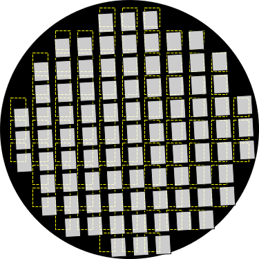
Debbie: When processing traditional eWLB (embedded Wafer Level Ball Grid Array) FO, there are two common issues, which are die shift and warpage. Die shift is a prevalent issue that highly affects yield. It happens when the die location has an offset from where it is designed to be, which is typically caused by die placement accuracy plus mold flow during the molding process. Mold flow, if systematic, can be compensated for, but die shift during the die attach process is highly dictated by the machine accuracy. To achieve low die shift, high accuracy die bonders are necessary, and they can be expensive.
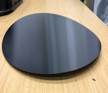
Warpage, on the other hand, is the result of the mismatched coefficient of thermal expansion of different materials, like mold compound and silicon. This leads to two different issues in manufacturing: One is yield, and the second is handling, which means you cannot process the wafer from the first step to the next step and so on. Every time a new layer is added onto the wafer, and every time the wafer goes through a certain thermal treatment, the warpage profile changes, and with the different magnitudes of warpage, the machines cannot handle the wafers. This means that you have to redesign your machine transport system, your handling system, and your end-effectors to allow this varying magnitude of warpage and also warpage profiles.
It’s a problem of continuous processing. It requires more operator intervention into the machine, and you risk equipment errors due to warpage, most typically vacuum failures of the chuck and end-effector. Warpage can also lead to issues in the photolithography process. If the wafer isn’t laying flat on the chuck, you can have issues of scumming, causing shorting in chips on the outer edge of the wafer, which results in lower yield.
Q: Since you joined ERS almost three years ago, you have been driving the development of machines to reduce the effects of warpage. What solutions does ERS offer that address the challenges you just talked about?
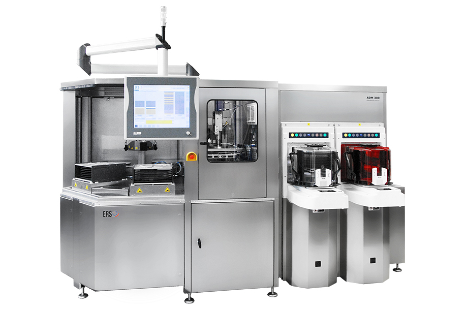
Debbie: My team and I have developed a wafer-level thermal debonding machine called ADM330 (Automatic Debonding Machine 330). It eliminates handling induced warpage in the debonding process by applying ERS Tri-temp slide technology. Thermal Debonding is a starting point for the layer build-up process. If you take eWLB as an example, the process that suffers warpage is the photolithography process. This process, aside from handling issues, will encounter yield problems when warpage is not minimized.
We have now extended this Tri-temp technology to different FOWLP layouts in a joint research project together with IME (Institute of Microelectronics) in Singapore.
Q: What were the findings from the research project with IME?
Debbie: Our study with IME targets to reduce warpage in 1.6 Fan-out ratio. Based on several customers’ experiences, you can get warpage in the range of 2-3 mm at a Fan-out ratio of 1.6. IME helps us dive into what the warpage impact is, which temperature works well with the warpage adjustment, and how we can solve this in our machine. As we know, the density of silicon in the wafer affects the warpage significantly. The closer the packaging area is to the chip area, the less mold compound to manipulate, the higher is the tendency of larger warpage. Using the sample created by IME together with our “Shock and Lock” method, we were able to achieve less than 1.5 mm warpage in 1.6 Fan-out ratio.
Q: As an important part of the semiconductor process, Advanced Packaging technologies need to break boundaries to keep up with the fast-developing market. Artificial Intelligence, 5G, IoT are some of the big buzzwords being used. What role does Fan-out play in these market trends?
Debbie: With the advantages like high-density I/O, good electrical performance, and so on, Fan-out is becoming the ideal technology to address the development of 2.5D/3D-stacking, Chiplets… Companies like Samsung, Intel have already started exploring the Chiplet space, for which Fan-out provides a competitive solution.
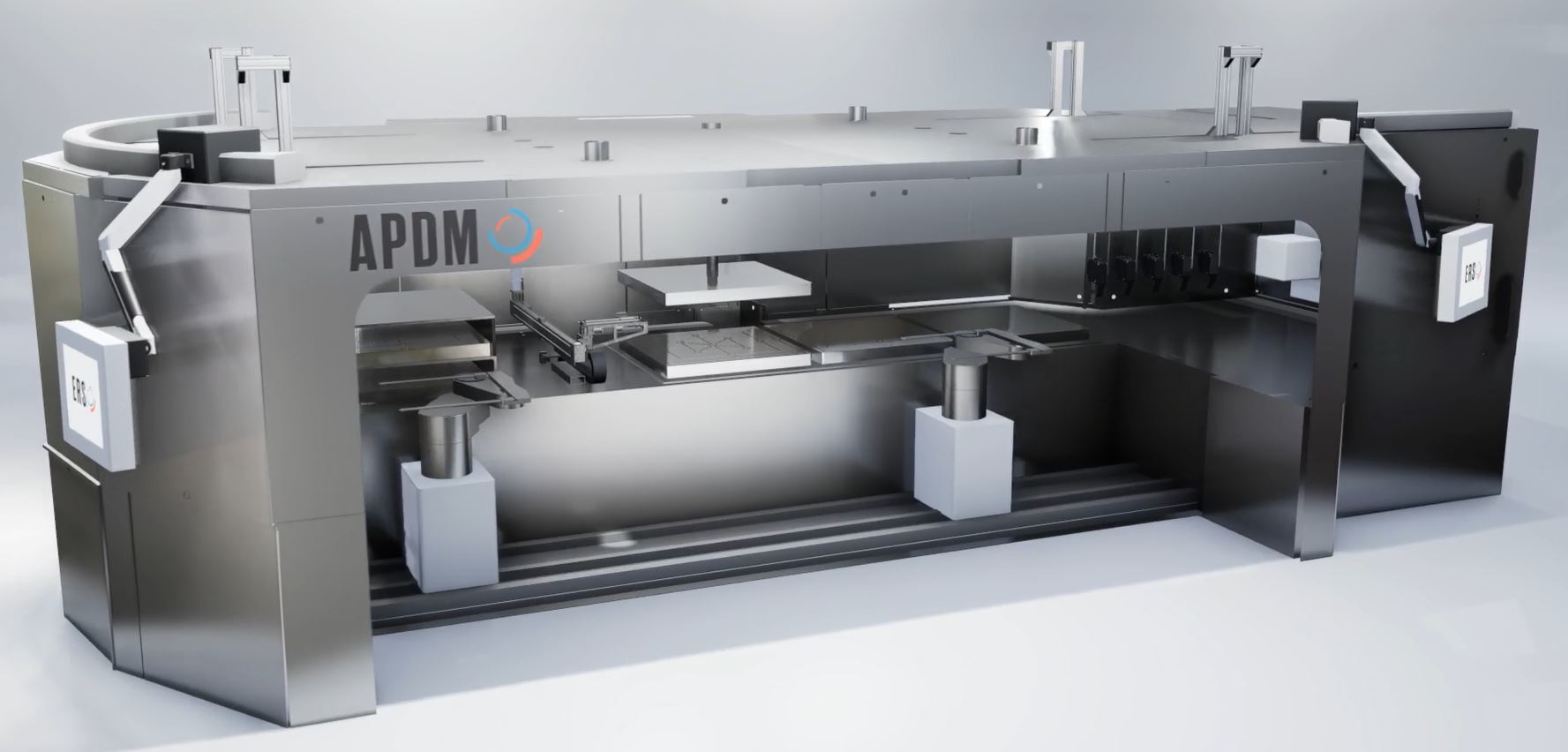
We see more and more industry players adopting Fan-out packaging. At ERS, we are developing solutions for larger formats and enhancing our warpage adjustment ability on more complicated Fan-out, such as multi-chips and other types of SiP. We are also ready for Fan-out Panel-Level Packaging (FOPLP). In 2018, we launched the first manual thermal debonding machine for panels up to 650x550mm. Its automatic version, called APDM, is in development and will be released later this year.
Want to know more about our Fan-out Equipment technologies? Click here to request a quote or send us your question via the contact form. And don’t forget to follow us on LinkedIn to get the latest news and updates from our company!