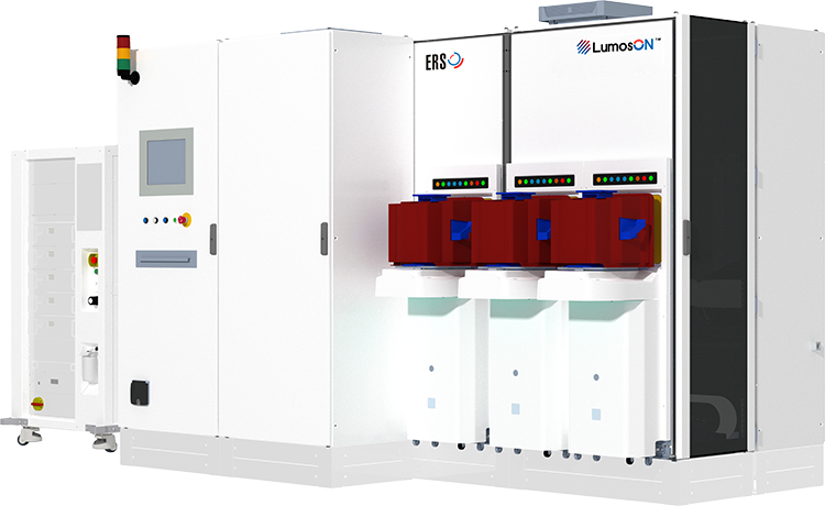
PhotoThermal debonding
Discover ERS’s PhotoThermal Debonding Technology, designed to deliver unparalleled flexibility, cost-savings, and high throughput for temporary bonding and debonding processes. This innovative, zero-stress debonding method allows for seamless processing independent of adhesive material type and supplier, ensuring adaptability in diverse production environments. The PhotoThermal process not only reduces operational costs but also significantly enhances production efficiency, making it the ideal solution for high-volume manufacturing of advanced semiconductor applications.

Technology Overview
Temporary bonding and debonding processes are vital in semiconductor packaging for both wafer thinning and fan-out technologies. They enable the manipulation of thin wafers during fabrication, ensuring structural integrity and facilitating advanced packaging techniques.
Temporary bonding supports the handling of ultra-thin wafers during thinning processes, while also holding redistributed chips in place during fan-out packaging. In addition to facilitating the handling and manipulation of thin wafers, wafer debonding is particularly critical as it allows for the separation of the carrier substrate from the thinned wafer or redistributed chips, enabling the finalization of the packaging process. This step is essential for achieving the desired package thickness, ensuring optimal electrical performance, and enabling further downstream processing steps such as redistribution layer formation and solder ball attachment.


ERS’s PhotoThermal debonding process allows stress-free debonding of temporary bonded wafers from a carrier. Stress-free debonding is made possible with a unique process and carrier combination approach. The energy is delivered by a flash lamp with the light absorbed by a light absorbing layer (LAL) in the carrier which converts light energy to thermal. This eliminates the adhesive material attached to the LAL and debonds the wafer safely. These processes enhance yield, throughput, and flexibility in packaging design, ultimately driving innovation in the semiconductor industry.
Why PhotoThermal Debonding?
Zero force, zero stress separation
PhotoThermal debonding is a stress-free debonding method, thanks to the special glass carrier, which converts the light from the controlled flash lamp to heat, thereby allowing the separation of carrier and wafer.
Reusable carrier
The carrier with light absorbing layer (LAL) can be reused up to 15 cycles without reapplying LAL.
No tape residue on carrier
The thermal energy resulting from the light absorption eliminates the bonding material, so no tape residue is left on carrier after debonding.
High tolerance for warped substrates
PhotoThermal debonding is also suitable for warped substrates, as there is no stress or force inflicted on the wafer during processing
Compatible with different bonding materials and suppliers
ERS has extensively tested and evaluated the most common bonding materials and suppliers to ensure that they are compatible with PhotoThermal debonding
Reduce process steps and complexity
Thanks to the special carrier, additional adhesive release layer coating together with the bond layer is not needed, thereby reducing process steps
>30% lower cost
Compared to laser debonding, PhotoThermal debonding can save more than 30% in operation costs


