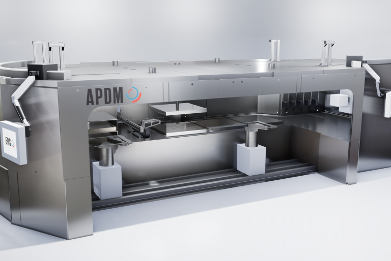
ERS electronic, the industry leader in the market of thermal management solutions for semiconductor manufacturing, is adding the Automatic Panel Debond Machine 650 (APDM650) to its portfolio of equipment for Advanced Packaging. ERS’s Manual Panel Debond Machine (MPDM), quickly gained traction in the industry after it was announced in 2018, and remains the leading solution among research and development and New Product Introduction teams.
With the APDM650, ERS takes it a step further. It features ERS’s renowned Thermal Debonding technology and Warpage Adjustment capability which includes the patented TriTemp slide technology that eliminates handling induced warpage. Its efficient automatic debonding and detaping process results in zero tape residue and no excursion. With its contactless transport mechanism, the warpage output can be as low as 4 mm. The machine’s design also enables a high degree of flexibility. The 650 x 650 mm chuck dimension can be used for different panel sizes, and the loading and unloading mechanism can be customized according to the customer’s different EFEM configurations. Combined with an industry-best temperature uniformity of ±3°C (at operating temperature of 185°C), ERS’s APDM650 is the perfect tool for high volume manufacturing on large panel format.
“Driven by the aim for further miniaturization and cost competitiveness, we see high growth in the Advanced Packaging market, and a surge in demand for FOPLP solutions,” says Laurent Giai-Miniet, CEO and CSMO of ERS electronic. “Following the successful introduction of our MPDM in 2018, the release of the APDM650 demonstrates our continuing commitment to this market.”
“The APDM650 combines everything we’ve learnt from the past 15 years of working with thermal debonding and warpage correction. The result is a comprehensive machine with an established production process that is designed to tackle the biggest challenges related to high volume large format manufacturing,” says Debbie-Claire Sanchez, FO Equipment Business Unit Manager at ERS electronic.
“For large area FOPLP, debonding is a crucial step to the process integrity of the panels,” says Dr. Tanja Braun, Group Manager of Fraunhofer IZM and Head of the Panel Level Packaging Consortium. “Working with the manual debonder MPDM of ERS at Fraunhofer IZM since 2018 has taken FOPLP process development a big step further in that regard. It is exciting to see that PLP has now reached technical and process maturity and is ready for high volume manufacturing.”

