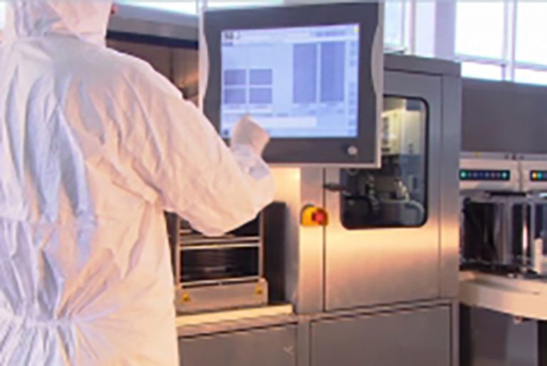
One and a half years after its launch, ERS electronic GmbH’s FOWLP (Fan-out Wafer Level Packaging) competence center near Munich (Germany) is being utilized by an increasing number of semiconductor chip makers, research institutes, materials suppliers and packaging sub-contractors. The ERS lab provides the opportunity to utilize ERS’ latest tools for production processes associated with eWLB (embedded Wafer Level BGA) and other FOWLP applications. The applications now being supported by ERS tools and engineers are more diverse than ever – some even include processes normally covered by more conventional front end tools. This increased participation in new development projects and the corresponding use of the ERS competence center is particularly pronounced in the second half of 2012.
“We are more than pleased with the acceptance of our offering throughout the entire industry and around the world”, said Klemens Reitinger, Managing Director of ERS. “Besides being utilized by third parties and new customers it also strengthens the ties to our existing customer base.”
The competence center creates a win-win situation for both the partners it supports and for ERS electronic: While delivering access to its patented debonding and warpage control technology, ERS keeps itself informed on emerging customer technologies and requirements. This means that ERS has the information it needs to stay ahead of the curve and be in a position to design, develop and deliver FOWLP equipment for upcoming packaging processes in a timely way.
“No matter which direction the technological development goes, thermal processing will be a strategic element present in all processes”, Reitinger said.

