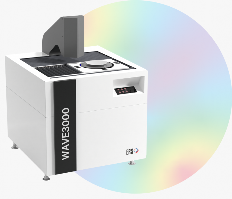
Wave3000
Introducing Wave3000, the revolutionary contactless 3D wafer profiler that employs advanced optical scanning technology to accurately measure wafer deformities in three different platforms (patent pending). With its state-of-the-art features, Wave3000 provides a comprehensive and precise analysis of wafer warpage, which is crucial for ensuring the quality of semiconductor devices.

Description
The ERS Wave3000 uses a high-resolution optical scanner that captures surface data of the wafer at multiple points, enabling it to generate an accurate 3D map of the wafer contour. The system’s advanced software algorithms then analyze the collected data to accurately calculate the wafer’s warpage profile, including variations in the curvature or wafer deformity.
What sets Wave3000 apart is its interactive 3D view of the wafer, which provides a better understanding of the warpage profile. The 3D view can be rotated and zoomed in, allowing users to view the warpage profile from any angle and assess its impact on the wafer’s performance. Additionally, Wave3000’s software can generate reports and graphs that help users interpret the measurement results and make informed decisions.
Wave3000 is easy to use, with a user-friendly interface that allows for quick and efficient measurement setup and execution. The tool’s contactless operation also reduces the risk of contamination and damage to the wafer, ensuring that the measurement results are accurate, safe, and reliable.
Wave3000
Technical data
Flat-surface vacuumed
3-pin position
End-effector placement
.csv file
Dimensions
Facility Supply
*e.g. silicon, mold compound, and others.
For special requirements, please contact us.
